How to Make a DC-DC Converter?
For electronics enthusiasts, successfully building a DC-DC converter is a deeply rewarding experience. It not only provides a deep understanding of the core principles of switching power supplies but also provides a stable power source for future projects. This article will guide you through the construction of a basic non-isolated step-down (Buck) converter.
Basic Principles of DC-DC Converter Construction
The core principle of the buck converter we will build is pulse-width modulation (PWM).
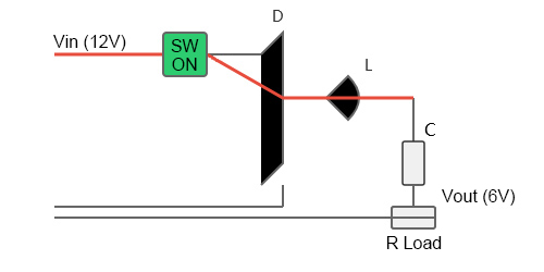
Switch-On Phase
When the switch (MOSFET) is closed, the input voltage is connected to the circuit. Current flows through the inductor, which begins to store magnetic energy, charging the output capacitor and supplying power to the load. At this point, the diode is reverse-biased and cuts off.
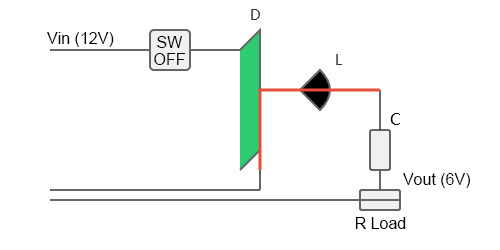
Switch-Off Phase
When the switch is turned off, because the inductor current cannot change suddenly, it generates a reverse electromotive force to maintain the current flow. At this point, the inductor becomes a power source, releasing energy through the freewheeling diode, continuing to supply power to the load and maintaining the output voltage.
Voltage Regulation
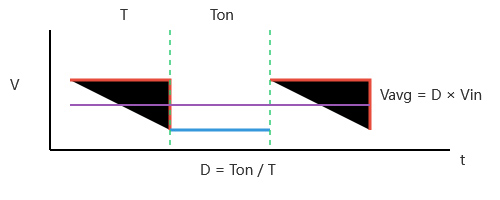
By controlling the ratio of the switch on-time (pulse width, Ton) to the total switching period (T), or the "duty cycle" (D = Ton / T), we can control the average energy delivered to the load. For an ideal DC-DC buck converter, the output voltage Vout ≈ D × Vin. For example, if the input is 12V and a 6V output is desired, the duty cycle D should be controlled around 50%.
Materials for Building a DC-DC Converter
The following is a list of materials needed for a classic buck converter based on the TL494 PWM controller chip:
Core controller: TL494CN (a common push-pull output switching power supply PWM controller chip)
Switching element: N-channel MOSFET, such as the IRFZ44N (sufficient voltage and current rating, easy to drive)
Energy storage element:
- Inductor: A power inductor of approximately 100μH (must be able to withstand the expected output current; you can use a toroidal or I-shaped inductor to wind your own).
- Capacitors:
Input Filter Capacitor: a 100μF/50V aluminum electrolytic capacitor, a 0.1μF ceramic capacitor
Output Filter Capacitor: a 470μF/25V electrolytic capacitor, a 10μF multilayer ceramic chip ceramic capacitor
Freewheeling diode: Fast recovery rectifier diodes or Schottky diodes, such as the 1N5822 (3A, 40V) or MBR1645. Do not use standard rectifier diodes such as the 1N4007.
Feedback resistor: An adjustable resistor (such as a 10kΩ multi-turn potentiometer) and a fixed resistor (such as 1kΩ, 10kΩ) are used to set the output voltage.
Other components:
- Chip oscillator timing resistor (Rt) and capacitor (Ct): For example, Rt = 10kΩ, Ct = 1nF (determines the switching frequency, f ≈ 1.1/(Rt × Ct)).
- Bootstrap capacitor (optional, for enhanced drive): 10μF/25V.
Supporting Equipment:
- PCB (or multi-purpose board/perfboard)
- Heat sink (for MOSFET and diode)
- DC power supply (e.g., 12V input)
- Electronic load or power resistor (e.g., 10Ω/5W)
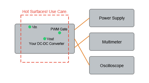
- Oscilloscope (optional, but extremely helpful for debugging)
- Multimeter
Detailed Steps for making a DC-DC Converter
Step 1: Circuit Design and Parameter Calculation
Calculate key parameters based on your input and output voltage/current requirements.
- Determine the duty cycle: D = Vout / Vin.
- Set the switching frequency: Select Rt and Ct, for example, set it to 50kHz.
- Calculate the inductor value: Use the formula L = (Vin - Vout) × D / (f × ΔIL), where ΔIL is the inductor ripple current, typically 20%-40% of the maximum output current.
- Set the output voltage: The TL494 receives feedback from the output through its internal error amplifier. A voltage divider network, formed by a potentiometer, compares a portion of the output voltage (usually half of Vout) with the chip's internal 2.5V reference voltage, dynamically adjusting the PWM to stabilize the output.
Step 2: Draw the circuit diagram and simulate
Draw the complete circuit diagram on paper or using EDA software (such as KiCad or EasyEDA). It is strongly recommended to perform preliminary simulations using simulation software such as LTspice to verify the correctness of the design and observe waveforms at key nodes.
Step 3: PCB Fabrication
Convert the designed circuit diagram into a physical circuit board. You can fabricate it yourself using thermal transfer printing, or send the design files to a PCB fabricator for small-batch production. For prototyping, soldering on a multimeter board is also feasible.
Step 4: Component Soldering
Following the principle of "lower components first, higher components later," solder small components such as resistors and diodes first, then chip holders and capacitors, and finally MOSFETs and diodes that require heat sinks.
Important Notes:
- Pay attention to polarity: The pin orientation of electrolytic capacitors, diodes, and MOSFETs must be correct.
- Ensure that solder joints are smooth and secure to avoid cold solder joints and short circuits.
Step 5: Pre-Power-On Inspection
- Visual Inspection: Carefully verify the correct values and orientation of all components.
- Multimeter Inspection: Use the diode or resistance setting on your multimeter to check for short circuits at the power input. Confirm that there are no short circuits before proceeding to the next step.
Step 6: Power-On and Testing
- Low-voltage, no-load test. Use an adjustable power supply, set the voltage to around 5V, and set a low current limit (e.g., 100mA). Turn on the power and observe the circuit board for any abnormal heating or smoke.
- Check the core voltage. Use a multimeter to measure the TL494's Vcc pin for voltage and the reference voltage output pin (usually pin 14) to see if it outputs a stable 5V. Measure the PWM output pin for voltage fluctuations.
- Gradually increase the input voltage. If there are no abnormalities, gradually increase the input voltage to the rated value (e.g., 12V). At this point, you can still disconnect the load.
- Measure the output voltage. Use a multimeter to measure the output voltage and adjust the potentiometer to observe whether the output voltage changes linearly.
- Load test. Connect a light load (e.g., a 1kΩ resistor) to observe whether the output voltage is stable. Then, gradually increase the load to the rated value and monitor the output voltage stability with a multimeter.
Precautions for Building a DC-DC Converter
Safety First
When designing and manufacturing fundamental DC-DC converters, safety must always be the top priority. Extreme caution should be exercised regarding high voltage risks during operation. Even in low-voltage environments, stored charge in capacitors can be dangerous. Therefore, before debugging or modifying the circuit, ensure that all capacitors are fully discharged.
Furthermore, during load testing, components such as MOSFETs, diodes, and inductors may heat up rapidly. Avoid touching them directly to prevent burns.
Component Selection is Critical
Beyond safety regulations, component selection is crucial. For example, diodes must be fast-recovery or Schottky types. Conventional diodes have a long recovery time and cannot operate effectively under high-speed switching conditions, resulting in significant overheating and reduced efficiency.
Regarding capacitors, the equivalent series resistance (ESR) of the input and output capacitors is crucial. Choosing low-ESR capacitors helps filter high-frequency noise. Using ceramic capacitors in parallel with electrolytic capacitors is recommended for optimal performance.
Layout and Wiring
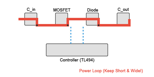
Layout and routing also affect overall performance. When routing, minimize the area of high-frequency loops, especially the high-frequency, high-current loop formed by the input capacitors, MOSFETs, and freewheeling diodes, to reduce electromagnetic interference and parasitic inductance.
In addition, special attention should be paid to the grounding method. It is recommended to separate the power ground and signal ground, and finally make a single-point connection at a location such as the negative terminal of the input capacitor to effectively suppress ground noise.
Debugging Tips
After completing the initial construction, proper debugging techniques can help quickly identify problems.
- If the circuit has no output, check the power supply connection, chip power supply, reference voltage, and MOSFET drive signal.
- If the output voltage is unstable or the ripple is excessive, focus on the feedback network connection, the quality and layout of the output capacitors, and the matching of the inductor values.
- If the component is abnormally hot, confirm that the MOSFET drive voltage is sufficient, the diode is correctly selected, and rule out overload.
Building a DC-DC converter is a process that closely integrates theory and practice. While the first attempt may not be perfect, every debugging and problem-solving experience is a valuable learning experience. Visit the ATO industrial automation platform for more professional technical support.
